A Schottky diode is a unilateral, metal-semiconductor device, with a low forward voltage drop and fast switching capabilities. Its characteristics are almost similar to those of the conventional PN diode. However, the Schottky diodes have superior properties such as the low forward voltage drop, fast switching in addition to producing less noise.
They are widely used in fast switching applications, rectifier circuits, RF circuits, and other applications where standard diodes cannot provide the same level of performance.
Construction of Schottky diode
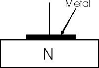
The construction differs from that of the standard PN-junction diode in that it uses a metal-semiconductor (M-S) junction known as the Schottky barrier. Majority of the junctions comprise of either platinum, chromium, molybdenum or tungsten metal as the anode and an N-type silicon semiconductor material as the cathode.

Fig 1 Basic Schottky barrier diode structure
Only one type of charge carrier is responsible for current transmission in Schottky diodes. The current across the metal-semiconductor junction is due to majority carriers such as the electrons, moving across the barrier, from the semiconductor to the metal, by diffusion, thermionic emission, and tunneling mechanisms.
IT = IDiffusion+ IThermionic emission +ITunneling
The three mechanisms exists in the junction, however, only one, such as the thermionic emission in the case of Silicon and Silicon carbide Schottky diodes, becomes the dominant current transport mechanism.
The construction enables the diode to have a high current density that leads to low forward voltage drop and conduction losses. In addition, the diode does not accumulate reverse recovery charge during its conduction period and has therefore a zero reverse recovery time leading to its ability to switch rapidly.
Advantages of Schottky diodes
- Low forward voltage drop of between 0.2 and 0.3 volts that leads to power savings.
- Higher efficiency hence less cooling and smaller diode heat sinks
- Fast recovery times and high switching speeds
- Low junction capacitance
- High power density
Disadvantages of Schottky diodes
- The diodes have a higher reverse leakage current as compared to the standard diodes and this might have issues in some designs.
- The reverse leakage current increases with temperature and can cause thermal instability
- Limited junction temperature of between 125°C to 175°C compared to about 200°C for the normal silicon diodes
- Limited reverse voltage of about 100V maximum
- They are expensive
Schottky diode IV characteristics
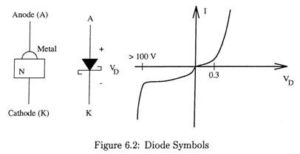
The IV characteristics are very similar for both the Schottky and the conventional PN diode; however the Schottky has a lower forward voltage drop of about 0.3 Volts.

Figure 2: Schottky diode IV characteristic
Key specification parameters
- Forward voltage drop: the voltage across the diode depends on the current and this is given at various current levels.
- Reverse breakdown: the diodes have lower breakdown voltage of less than 100 V. A ring guard ring is sometimes used to improve the reverse breakdown by a factor of about 4:1.
- The junction capacitance: this is specified at given voltages and is important for RF applications. The capacitance values are small in the order of a few picofarads.
- Working Temperature Tj: typically between 125 to 175°C
- Reverse recovery time: expressed in nanoseconds with typical values of about This is the time to change from forward conducting state to the reverse OFF state and is dependent on the capacitance.
- Reverse leakage current: increases with increase in junction temperature.
- Maximum Peak Current
- Maximum Average Rectified Current
Types of Schottky diodes
Silicon Schottky Diodes
The silicon diode has a low forward voltage drop hence lower conduction losses. However, the larger leakage reverse current is a challenge at higher temperatures.
Silicon Carbide (SiC) Schottky
Zero reverse recovery time and lower forward voltage drop but higher junction capacitance and greater leakage current compared to the conventional PN junction diode. The diode has a higher maximum junction temperature in addition to being thermally stable and unaffected by variations in the operating temperature. Typical ratings are maximum breakdown voltage of 1700 Volts and maximum forward current of 25 A.
Gallium Arsenide (GaAs) Schottky Diode
GaAs Schottky diodes have the lowest junction capacitance, are thermally stable, and capable of operating at 5 MHz and higher. It is available at a maximum breakdown voltage of 300 V and a maximum forward current of 29 A.
Applications of Schottky diodes
The diodes are used in a wide variety of applications ranging from rectifying to high speed logic circuits. Some of these include:
- Ultra-high speed switching
- Voltage Clamp circuits
- Rectifiers in power supplies circuits
- Power OR circuits
- RF applications
- In stand-alone photovoltaic systems
Summary
Schottky diodes have the desirable, ideal diode features in terms of forward voltage drop, junction capacitance, and reverse-recovery time that make them suitable for high speed switching and high frequency applications. However, their limited reverse voltage, high reverse leakage current, and low forward current make them unsuitable for some very high power applications.
Some newer developments such as the SiC and GaAs Schottky diodes are able to overcome some of these challenges, but their cost and limited documentation limit their use to only specific applications.